Cryogenic Qubit Integration
Superconducting circuits are most prevalently used in large-scale quantum computing. Since superconductor materials have substantially no electrical resistance below a certain critical temperature, they provide increased performance in integrated circuit devices, which can be used in a variety of electronic devices.
Researchers
-
shielded through via structures and methods for fabricating shielded through via structures
United States of America | Granted | 10,199,553 -
interconnect structures for assembly of semiconductor structures including superconducting integrated circuits
United States of America | Granted | 10,396,269 -
qubit and coupler circuit structures and coupling techniques
United States of America | Granted | 10,134,972 -
interconnect structures and methods for fabricating interconnect structures
United States of America | Granted | 10,121,754
Figures
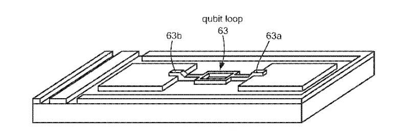
An aluminum qubit loop connecting two high-Q aluminum shunt capacitors on a Sapphire substrate. The qubit loop has three Josephson junctions, two on one side of the loop, and one on the opposing side.
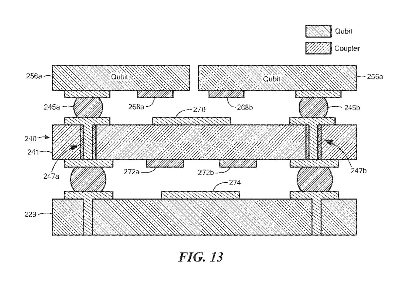
Inter-chip qubit coupling. A pair of quantum bit integrated circuits 256 are coupled to multi-chip modules 229 through a TSV substrate 240. Signals are coupled from qubit chips through superconducting interconnects 245 and signal paths 247
Technology
This technology is a cryogenic bit package comprised of quantum bit integrated circuits, a quantum bit bias control line, a superconducting multi-chip module, and superconducting interconnects to electrically couple the qubit circuits to the multi-chip modules. The interconnect structure is formed on a semiconductor structure with a resistive substrate and an interconnect pad, which together, allow for assembly of multi-layer semiconductor structures with multiple superconducting integrated circuits. This multi-layer semiconductor structure has a series of coupled interconnect sections that use superconducting qubit ICs to perform fast and nearly loss-less operations for quantum computer architectures. The interconnects of this system demonstrate minimal resistance in the superconducting path as well as efficient heat dissipation in the thermally conducting path.
Problem Addressed
To achieve the high computation speeds that meet the demands of higher functionality in integrated circuits while being pushed into smaller footprints, new packaging structures need to integrate more dies with greater function, higher I/O counts, and smaller die pad pitches. The current solutions for densifying packages are based upon materials selection, package design, and integration approach. This technology identifies material selection, package design, and integration approaches to minimize resistance for a superconducting path between two chips in a flip-chip configuration.
Advantages
- Stable interconnect with room temperature electronics.
- Increased I/O density for multi-qubit operations. Constitutive layer geometry supports long coherence times
Related Technologies
This case is related to MIT technologies: #18087, and #19039
Publications
Das, R. N., et al. "Large Scale Cryogenic Integration Approach for Superconducting High-Performance Computing," 2017 IEEE 67th Electronic Components and Technology Conference (ECTC), Orlando, FL, USA, 2017, pp. 675-683. doi: 10.1109/ECTC.2017.54.
Das, R. N., et al. "Cryogenic Qubit Integration for Quantum Computing," 2018 IEEE 68th Electronic Components and Technology Conference (ECTC), San Diego, CA, USA, 2018, pp. 504-514. doi: 10.1109/ECTC.2018.00080.
License this technology
Interested in this technology? Connect with our experienced licensing team to initiate the process.
Sign up for technology updates
Sign up now to receive the latest updates on cutting-edge technologies and innovations.