3D Cryogenic Packaging for Superconducting Computing
Superconducting computing offers an attractive low-power alternative to CMOS. Cryogenic packaging with 3D integration will allow superconducting computer circuits to fit within cryogenic chambers.
Researchers
-
interconnect structures and semiconductor structures for assembly of cryogenic electronic packages
United States of America | Granted | 10,242,968 -
cryogenic electronic packages and assemblies
United States of America | Granted | 10,586,909 -
cryogenic electronic packages and methods for fabricating cryogenic electronic packages
United States of America | Granted | 10,381,541
Figures
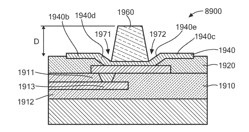
A semiconductor structure with interconnects and under bump metallurgy. The metal interconnect 1960 has a predetermined shape selected based upon an application of the semiconductor structure.
3D cryogenic integration approach shrinks superconducting computing hardware to small enough area to fit in cryogenic chamber
Technology
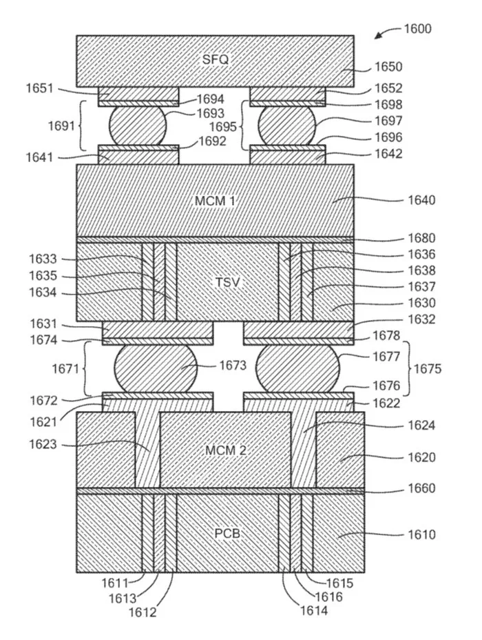
A superconducting computing architecture with a scalable cryogenic 3D integration approach is the solution to these requirements. This approach yields the ability to design computing circuitry to fit the cryogenic space, rather than adjusting the cryogenic space to fit the computer circuits. The cryogenic package includes multiple superconducting multi-chip modules, which connect to each other with room temperature semiconductor components. This structure allows the selection of the best possible, commercially available, superconducting die and components from various suppliers. The 3D design minimizes the use of physical space, and maximizes superconducting paths, to increase processing speeds and decrease signal path resistance.
Problem Addressed
In the realm of computing, superconducting integrated circuits greatly outperform CMOS with many advantages including faster switching speeds, low dissipative switching, and the use of small current pulses for information transfer. The major challenge is the lack of existing high performance integration schemes that meet the stringent requirements of cryogenic applications. Current technologies cannot provide an integration scheme that accommodates the thousands of single flux quantum chips needed for operation. Other requirements include high integration density per chip, a substantially miniaturized cryogenic cooling setup, low-resistance signal paths, and stability over cryogenic temperature ranges.
Advantages
- 3D cryogenic integration approach shrinks superconducting computing hardware to small enough area to fit in cryogenic chamber
- Decreased electrical resistance in signal path, increased processing speed
Related Technologies
This case is related to MIT technologies: #18087, and #18282
Publications
Das, R. N., et al. (2017). Large Scale Cryogenic Integration Approach for Superconducting High-Performance Computing. In 2017 IEEE 67th Electronic Components and Technology Conference (ECTC), Orlando, FL, USA (pp. 675-683). doi: 10.1109/ECTC.2017.54
Das, R. N., et al. (2018). Cryogenic Qubit Integration for Quantum Computing. In 2018 IEEE 68th Electronic Components and Technology Conference (ECTC), San Diego, CA, USA (pp. 504-514). doi: 10.1109/ECTC.2018.00080.
License this technology
Interested in this technology? Connect with our experienced licensing team to initiate the process.
Sign up for technology updates
Sign up now to receive the latest updates on cutting-edge technologies and innovations.