Novel Technique for Increasing Efficiency of 3DIC Fabrication
Multi-layered devices can be used in military and commercial applications, which includes sensor processing, mission data recording, communication, and flight electronics. 3DICs can also be implemented in portable consumer electronics like cell phones, tablets, and computers.
Researchers
-
multi-layer semiconductor structure and methods for fabricating multi-layer semiconductor structures
United States of America | Granted | 10,229,897
Figures
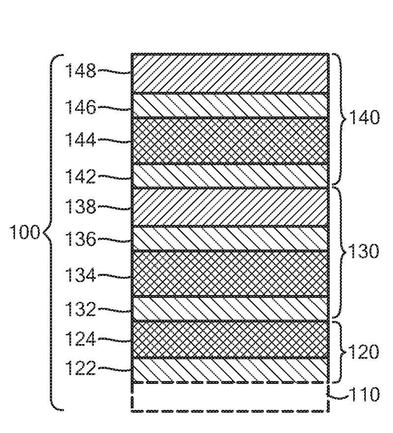
An example semiconductor stack featuring a plurality of sections. The sections have an insulating layer and a functional layer that alternate to prevent electrical shorts.
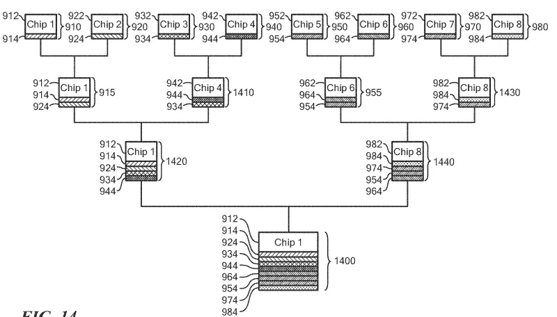
Advantage of parallel approach. Schematic shows 3DIC fabrication approach to reduce total bonding cycles and fabrication cycle time.
Technology
This technology covers multilayer semiconductor devices and methods for fabricating a multi-layer semiconductor structure. A simultaneous fabrication of building blocks, and subsequent alignment, joining and interconnection through a via last or via first process generates a multi-layer semiconductor structure. This fabrication approach provides the thinnest possible active area cross section for a multi-tier, flip-chip capable, hybrid, 3DIC. Thin cross-sections lead to lighter and slimmer 3D structures, so packaging can be more efficient. The integrated circuit has a total 2n stacked chips where “n” is the number of bonding cycles. This method uses the minimum number of bonding steps and shorter cycle times to fabricate 3DIC since each bonding of an individual chip or chip stack uses single side bonding. The insulating layers are made of a multilayer oxide having at least one chemically activated, ultra-smooth bonding surface capable of bonding to another surface without any external force. This surface bonding technology, combined with the minimized number of bonds, lowers the cost of manufacturing the 3D stacked circuits.
Problem Addressed
The trend toward miniaturization of electronic products necessitates smaller and more densely packed semiconductor structures. This has resulted in a demand for semiconductor packages which are relatively low loss, lightweight structures and which support increased electronic capabilities like increased density, mobility, and operational life. One solution to this demand is multilayer semiconductor structures or 3D integrated circuits. Fabricating these structures has been a costly and inefficient process since drilling through the insulator substrate can cause fracture and the final semiconductor product generally has worse performance than the 2D integrated circuit. Current 3D fabrication techniques have low processing speeds, high manufacturing costs, and take exorbitant amounts of time to create. The present devices and method promote reduced cycle times, cost-effective stacking alternatives and increased circuit efficiency.
Advantages
- Possible increase in power performance through interconnect length reduction and proper die placement
- An increase in chip stacking without the cumulative yield loss of sequential processing
- Reduced fabrication cycle time
Related Technologies
This case is related to MIT technologies: #17313, #17465, and #16918
License this technology
Interested in this technology? Connect with our experienced licensing team to initiate the process.
Sign up for technology updates
Sign up now to receive the latest updates on cutting-edge technologies and innovations.