High Consistency and High Yielding Resistive Switching Devices.
Resistive switching (RS) devices are actively pursued by semiconductor industries for next generation resistive RAM. RS devices will soon replace transistors as fundamental units in next-generation computer circuits. Large scale RS arrays are used in machine learning applications, hardware neuromorphic networks, and hardware-implemented matrix multiplications.
Researchers
-
techniques for dopant implantation and multilayer oxides for resistive switching devices
United States of America | Granted | 11,201,285
Figures
Technology
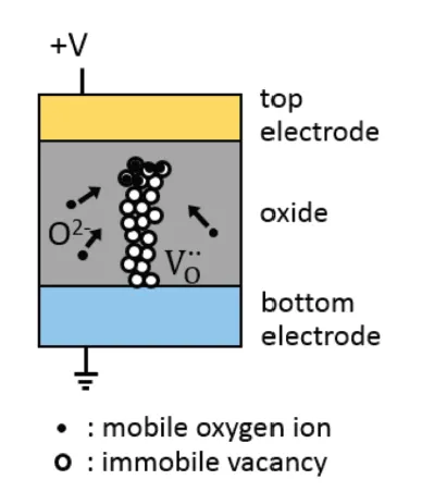
This resistive switching device combines multiple technologies in a way that revolutionizes the field of RS devices. A simple RS device consists of a top electrode, an oxide material, and a bottom electrode. RS behavior comes from the formation and dissipation of an oxygen vacancy filament between these layers. Certain processing factors are paramount in achieving good switching characteristics that have not been identified in the prior art. Factors affecting device behavior include material choices for the electrodes and oxide as well as thicknesses of individual layers. Other control parameters can be tuned when integrating RS devices into large arrays. For example, doping is a rich tuning parameter as it grants the choice of dopant material and doping profile/distribution. Gold metal dopants improve switching consistency and eliminate the need for a low-yield electroforming step during fabrication. Another strategy is fragmentation of a thick oxide layer into multiple thinner oxides. This lifts the restriction of needing to find different, but suitable, oxide materials to tap into the benefits of using multilayer films. The multiple oxide layers significantly improve consistencies across cycles and across devices while sharpening the LRS to HRS transition. These features are important for achieving good switching characteristics.
Problem Addressed
An ideal RS device operates reversibly and has consistent switching behaviors for each cycle. The challenge in producing marketable dual purpose computation and memory units lies in the poor device yields and inconsistent switching behavior of the RS unit. The poor yields and device variations arise from the stochastic nature of the formation of filaments in the insulating dielectric layer structure, causing I-V curves to differ substantially between cycles and between devices. The cycling between high resistance states (HRS) and low resistance states (LRS) can also terminate abruptly via a permanent breakdown of the dielectric layer.
Advantages
- Improved switching consistency with sharper transitions between low resistance and high resistance states
- High device fabrication yields and switching consistencies, both across cycles and across devices; lowers manufacturing costs due to less wasted material
License this technology
Interested in this technology? Connect with our experienced licensing team to initiate the process.
Sign up for technology updates
Sign up now to receive the latest updates on cutting-edge technologies and innovations.

