Engineered Carbon Nanotube Stamp for High Performance Micro-Contact Printing
Direct printing methods provide cost-effective routes for manufacturing of functional devices in large-area and unconventional formats. In particular, industrial printing technologies including screen, inkjet, gravure, and flexography, are essential to current and future manufacturing of microelectronics on flexible substrates, including displays, circuits, photovoltaic (PV) arrays, and radio frequency identification (RFID) tags. These printing techniques can rapidly reproduce 2D patterns of functional inks (e.g., metal nanoparticles, organic optoelectric materials) onto flat, curved, flexible and stretchable substrates.
Researchers
-
nanoporous stamp for flexographic printing
United States of America | Granted | 10,118,426 -
nanoporous stamp printing of nanoparticulate inks
United States of America | Granted | 10,583,677 -
nanoporous stamp for flexographic printing
Patent Cooperation Treaty | Published application
Figures
Technology
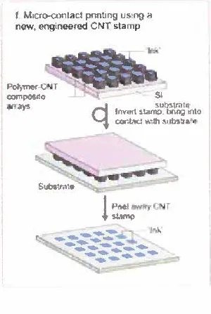
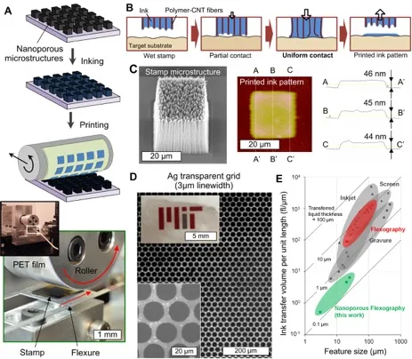
The inventors have developed a new class of stamp material composed of vertically aligned multi-walled carbon nanotubes (CNTs) conformally coated with functional polymers. A thermal chemical vapor deposition (CVD) process is used to grow patterned CNT arrays on silicon substrates, forming vertically aligned “forests” or “arrays” where the individual CNTs are perpendicular to the substrate. The top layer of the CNTs is removed by plasma treatment, which reduces the surface modulus and enables conformal contact against the target substrates. The individual CNTs within the arrays are coated with functional polymer films, such as poly-perfluorodecylacrylate, p(PFDA), by initiated chemical vapor deposition (iCVD) process. This conformal p(PFDA) coating is an average thickness of 30 nm and ensures the microstructures do not shrink or collapse after wetting and dewetting. Finally, the polymer coated CNT arrays are plasma-treated again to control the surface wettability. This new stamp microstructures are highly porous (>90% porosity), wettable with colloidal inks but mechanically durable against capillary shrinkage, and yet compliant enough to enable conformal contact during flexographic printing. As a result, the stamps enable direct printing of liquid inks with micrometer lateral resolution which surpasses the resolution limit of undustrial flexography technology by >10-fold.
Problem Addressed
Lateral resolution of conventional printing methods is in general limited to 10-100 µm, which remains as a main challenge toward high performance electronics. For example, inkjet is limited by the size of the droplet ejected from the nozzle aperture; due to the limiting strength and frequency of transducers compared to the force required to eject smaller liquid droplets. The resolutions of screen printing and gravure are strongly restricted by the key geometrical parameters of printing tools, such as the woven mesh openings in screen printing stencil and volume of the engraved cells in gravure cylinder. Although elastomeric stamp features can easily be reduced to nanometer range using replica molding techniques, flexography is also limited because of the contact-mediated liquid instabilities and spreading.
Advantages
- Direct-printing allows for low-cost, rapid and mass production capabilities
- Nanoporous stamp can be sized to sub-micrometer scale while retaining mechanical robustness
- Direct printing of electronic nanomaterials with few micrometer lateral resolution
- Engineered for automated, mass production systems for high throughput production
- Far-ranging applications including repeatable liquid printing, electrical micro-contact printing, and tunable wettability/adhesion of stamp surface depending on coating
Publications
Sanha Kim, et al. "Ultrathin High-Resolution Flexographic Printing Using Nanoporous Stamps." Science Advances 2 (2016): e1601660. doi: 10.1126/sciadv.1601660.
License this technology
Interested in this technology? Connect with our experienced licensing team to initiate the process.
Sign up for technology updates
Sign up now to receive the latest updates on cutting-edge technologies and innovations.

