Dielectric Technology for Nitride Semiconductor Devices
Many applications of GaN-based high electron mobility transistors (HEMTs) require reliable operations at high levels of power and temperature while maintaining a low leakage current. This invention can be used in technologies such as microwaves and power switches as well as in large-scale applications for advanced transportation systems, energy delivery networks, and electricity conversion.
Researchers
-
dielectric technology for nitride semiconductor devices
United States of America | Granted | 10,297,456
Figures
Technology
The invention describes MOSFETs or Metal–Oxide–Semiconductor Heterostructure Field-Effect Transistor (MOSHEMTs) with GaN 9 or other N-containing semiconductor's device containing thermally oxidized polysilicon. The SiO2 dielectric layer is achieved through thermally oxidizing the N-containing semiconductor's Polysilicon layer that rests on top of the semiconductor. The resulting layer of SiO2 is a high-quality oxide with improved properties over deposited oxides that are produced by chemical vapor deposition. The final dielectric stack is comprised of this thermal SiO2 and a thin layer of native like Ga2O3 at the interface with the AlGaN polarizing layer, which results in a very low Interface States Density (Dit) values. Controlling the temperature of thermal oxidation gives better control of the oxidation rate of the silicon dioxide layer. Since SiO2 limits the rate of oxidation of the nitride semiconductor, one can decrease the rate at which oxidizing species that reach the nitride semiconductor by increasing the thickness of the deposited silicon.
Problem Addressed
Previous attempts at incorporating a dielectric layer to achieve low leakage at high power/temperature operation and improved reliability were unsuccessful in achieving the ideal combination of a large critical electric field and a good interface between the oxide and the semiconductor. The limited critical field of conventional transistors made of silicon leads to bulky commercial devices that operate at low frequencies and require high resistances. This invention creates a semiconductor interface within HEMTs that leads to gate stacks with low interface states density and large critical electric fields necessary for high power operations. This allows for the creation of reliable, high-efficiency power electronics.
Advantages
- GaN based MOSFET or MOSHEMT with low gate leakage and high reliability
- Stable and reproducible fabrication
- Easy incorporation into existing semiconductor processing techniques
Publications
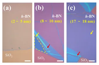
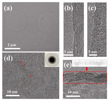
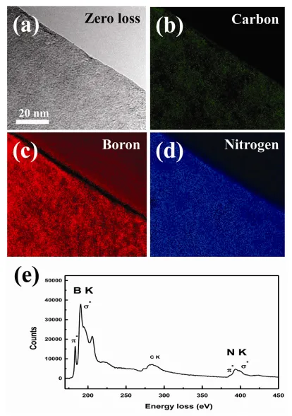
Kim, Ki Kang, et al. "Synthesis and Characterization of Hexagonal Boron Nitride Film as a Dielectric Layer for Graphene Devices." ACS Nano 6, no. 10 (2012): 8583-8590. doi: 10.1021/nn301675f
License this technology
Interested in this technology? Connect with our experienced licensing team to initiate the process.
Sign up for technology updates
Sign up now to receive the latest updates on cutting-edge technologies and innovations.


