Block Copolymers for 3D Printing
The combination of a crowded RF spectrum and the requirement for high-bandwidth communications has created a need for low-loss high frequency RF devices. High precision 3D printing of dielectrics offers improved device properties and performance and supports complex fabrication not traditionally possible with subtractive manufacturing. The technology can be applied to fully integrated GHz and THz devices, flexible electronics, and microfluidic devices.
Researchers
-
block copolymer ink formulation for 3d printing and method of making a 3d printed radiofrequency (rf) device
United States of America | Granted | 10,851,251
Figures
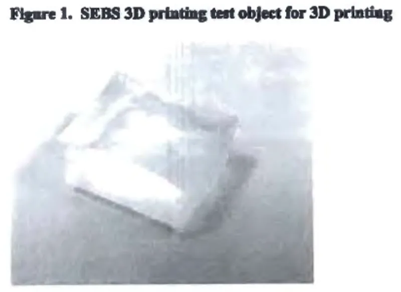
Example of a 3D printed object with exceptionally low loss values
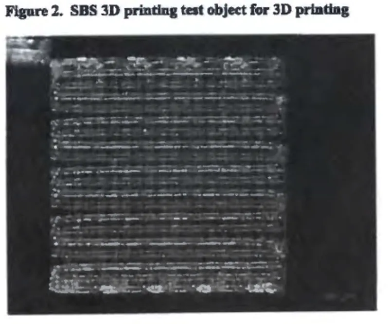
3D printed example of a dielectric material with low loss values

3D printed dielectric material with tailored dielectric properties and low loss values
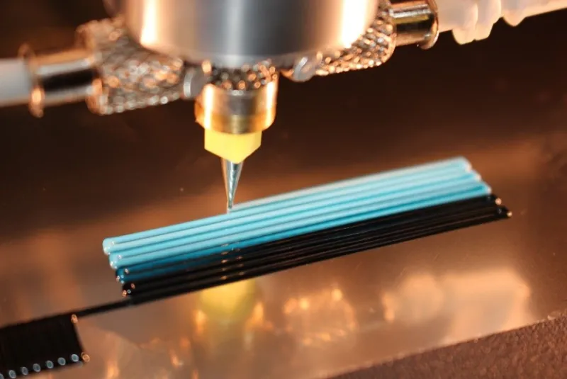
Photo of a printed dielectric with a gradual transition from one material to another
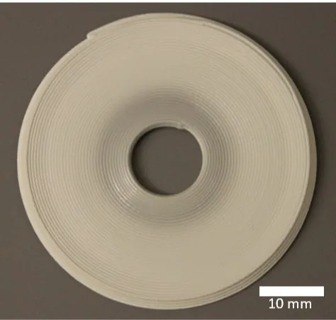
Printed dielectric substrate where the dielectric constant of the structure transitions from 2.2 to 24.5 in a radial pattern
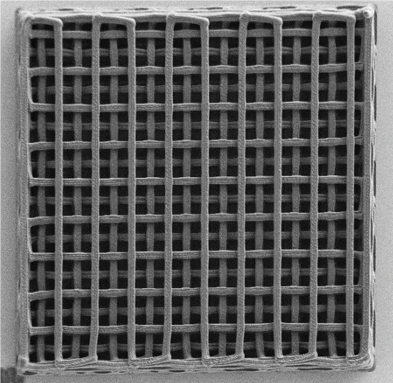
Printed log pile demonstrates the resolution of the printer with a 10 micron nozzle
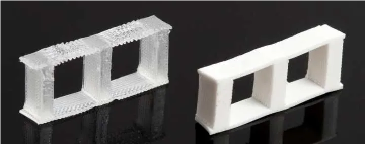
Two three-block filters with the same dimensions are pictured. The filter on the left is printed with pure SIS polymer. The filter on the right contains 26% Al2O3.
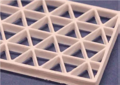
Triangle lattice printing demonstration to give a 57% by weight alumina structure
Technology
The invention describes an ink formulation and method of making a 3D printed RF device. The ink consists of a triblock copolymer in a solvent, and one or more additives that can enhance the flow of the ink and improve properties of the end structure, including dielectric properties. The ink is viscoelastic, allowing for greater control over the rate and method of flow. The ink can include dielectric filler particles that alter the RF properties in a predictable fashion while maintaining micron scale resolution. The method describes extruding an ink formulation from a deposition nozzle moving relative to a substrate, which can increase the range of geometries of 3D structures to be built layer by layer. One or more continuous filaments comprising the ink formulation can be deposited in a predetermined pattern on the substrate. Once printed, the ink formulation is treated to remove or cure the solvent, thereby forming a printed RF device. Notably, this materials system and printing process allows for the fabrication of devices whose properties can be tailored in a graded pattern avoiding abrupt interfaces within the part.
Problem Addressed
High resolution 3D printing has significant advantages for enhancing device performance and reducing size, weight and power (SWaP). However, applications thus far have been limited by the lack of appropriate materials and printing processes. Current fabrication methods are costly, offer limited material selection and are inflexible to customization. Machining the polymeric and ceramic materials used for high-frequency devices can be difficult and laborious.
Advantages
- Complex multi-layered structures direct from design
- Low loss polymer material printing with high resolution and low surface roughness
- Enhanced properties and performance for advanced RF devices
- Fabrication of devices not possible by conventional methods
- Radically improved efficiency of high frequency devices
Publications
Zai, A., et al. "Dielectric Nanoparticle-Laden Polymers for Millimeter-Wave 3D Printing." Technical Report presented at the 42nd Annual GOMACTech Conference (GOMACTech 17), March 20-23, 2017. Lincoln Laboratory, Massachusetts Institute of Technology, Lexington. (NTIS Issue Number 201805).
Lis, M., et al. "High Performance, 3D-Printable Dielectric Nanocomposites for Millimeter Wave Devices." ACS Applied Materials & Interfaces 8, no. 49 (2016): 34019-34026. doi: 10.1021/acsami.6b11643.
Lis, M., et al. "Polymer Dielectrics for 3D-Printed RF Devices in the Ka Band." Advanced Material Technologies 1, no. 2 (2016): 1600027. doi: 10.1002/admt.201600027.
Zai, A., Lis, M., Cipolle, D., Russo, J., Plaut, M., Fedynyshyn, T., & Lewis, J. "3D-Printed Millimeter Wave Structures."
License this technology
Interested in this technology? Connect with our experienced licensing team to initiate the process.
Sign up for technology updates
Sign up now to receive the latest updates on cutting-edge technologies and innovations.